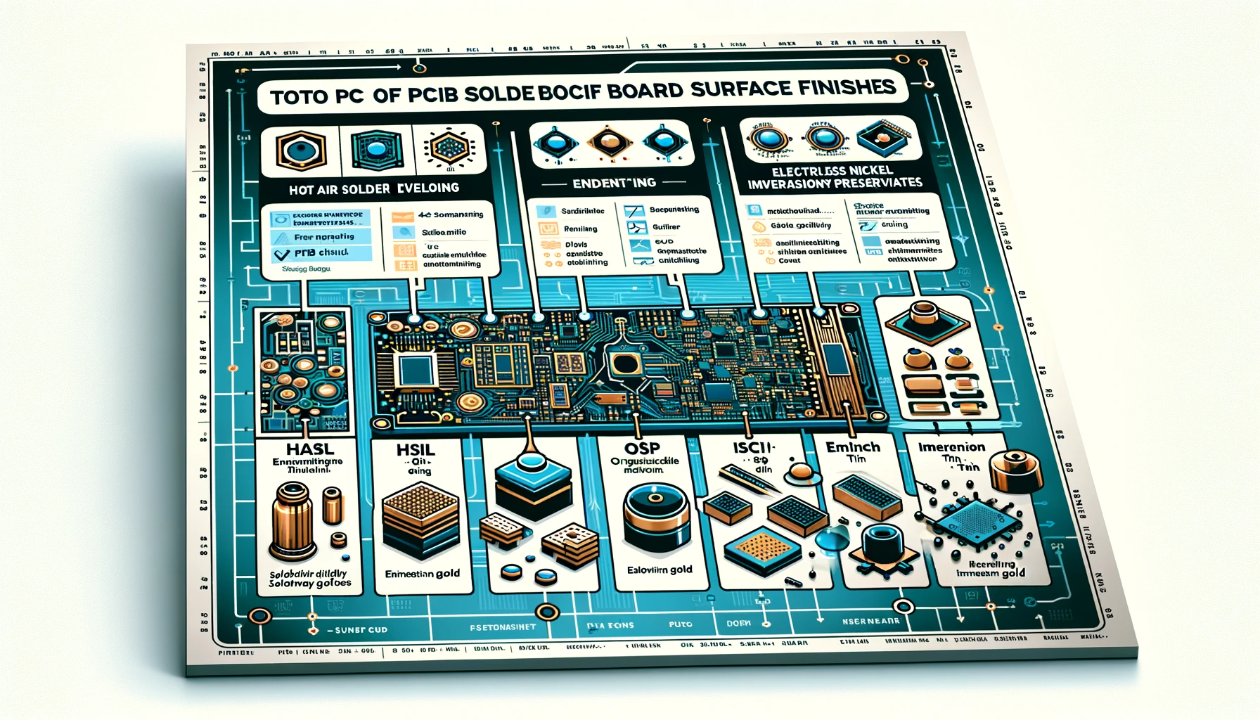
PCB Floor End Options Professionals & ConsPCB Floor end kind the crucial interface between the board and the parts. Lately, their widespread availability has overwhelmed some digital designers. This submit hopes to shed some gentle on the professionals and cons of the 4 most dominant PCB floor end options in the marketplace: Natural Solderability Preservative (OSP), Electrolysis Nickel Immersion Gold (ENIG), Electroplated Nickel Gold and Immersion Tin or Silver. The next submit applies to Inflexible Printed Circuits Boards (PCB) and Versatile Printed Circuit (FPC).Notice: PCBs are usually fabricated from inflexible supplies and won’t bend throughout their software. FPCs are normally skinny and fabricated from supplies able to bending and/or motion throughout software. Processing and software necessities dictate whether or not the PCB floor end is electroplated, electrolysis, immersion or deposited.
Circumstances that affect PCB Floor End Choice:
Oxidation safety of PCBs metallic traces (normally copper).
Floor solderability for electrical and mechanical part attachment.
Floor bondability for chip mounted parts utilizing gold and aluminum wire.
Mechanical functions (e.g. stress, strains and so forth.).
Environmental situations (e.g. temperature, relative humidity and so forth.).
Mechanical contacts requiring abrasion resistance and oxidation safety.
Common Dialogue of Accessible Floor finishes
Natural Solderability Preservative (OSP)OSP has a restricted shelf life. Its most frequent use is soldering when the protectant is dissipated through the course of, thus no extra removing processes are wanted.Warning: as soon as eliminated, the naked copper is uncovered and topic to oxidation. When a number of finishes are wanted on the identical PCB, OSP may be utilized over different kinds of floor end (e.g. wire bonding and soldering, mechanical contact surfaces and soldering, and so forth.).Electrolysis Nickel Immersion Gold (ENIG)ENIG is a extensively used floor end for soldering, aluminum wire wedge bonding and mechanical contact factors (connector pads, take a look at factors, and so forth.). The copper floor has an electrolysis nickel layer deposited (150 micro inches minimal) to seal the copper. A layer of gold is then deposited to guard the nickel from oxidation and supply a solderable floor to the nickel. The gold is absorbed and dispersed into the solder. The gold is an immersion course of and the thickness is self-limiting (2 to three micro inches max).The nickel layer may be very brittle and can’t be subjected to emphasize or strains within the Z axis with out cracking. Versatile PCBs are particularly vulnerable to this with all areas topic to potential bending supported with rigidizing supplies.Warning: Improperly managed ENIG processing may end up in weak solder connections which might not be seen and/or lead to failure. A typical signal of failure is a flat black copper pad after the connected part has been forcibly eliminated.Electroplated Nickel GoldIn at the moment’s complicated circuits, this floor end may be very restricted as a result of it requires that every one surfaces to be plated must be electrically related (i.e. {an electrical} cost have to be current for plating). These interconnections should then be damaged to make the circuit useful. The plated nickel may be very solderable and never topic to the solderability problems with ENIG. The plated gold has no limits on thickness and may assist wire-bonding processes like Thermo Compression Bonding (i.e. ball bonding).Warning: Thicker gold may end up in solder joints being too brittle when utilizing lead based mostly solders.Immersion Tin and Immersion SilverThese processes present solderable surfaces however are likely to have oxidation and tarnish points that affect solderability. They don’t seem to be extensively used or obtainable.
A latest research indicated that the careers of a number of mid-level IT engineers are at peril. Selections taken by corporations, feedback by business tycoons and statements by business analysts…
MS Outlook is taken into account as one of the most well-liked E mail utility that’s broadly used for receiving and sending mails. To retailer all of the despatched,…
A website is a must-have in today’s digital age of doing business. However, not all websites can deliver the anticipated benefits. Web design is a complicated area to navigate….
Samsung be aware Eight is slated to be launched in 2017. Additionally, as a result of renewed battery, it stays to be seen if it has a better battery capability…
If you’re one of the millions of people now working from home, you’ve probably been using your laptop more than ever. You’re ready for an upgrade! Here’s some unexpected advice:…
This concept was conceived attributable to the truth that so many individuals use their smartphones for various issues together with enterprise. That is each day and all of us like…